Harnessing DNA to make cutting-edge nanoscale semiconductors
[[{“value”:”
Harnessing DNA to make cutting-edge nanoscale semiconductors
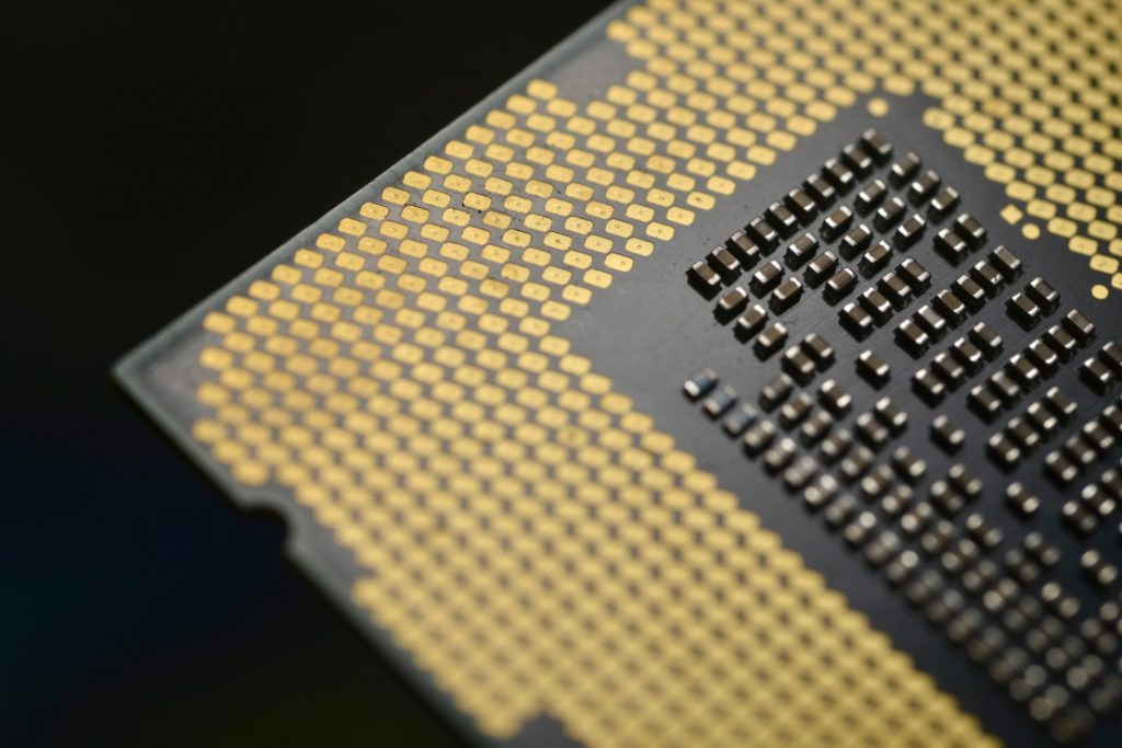
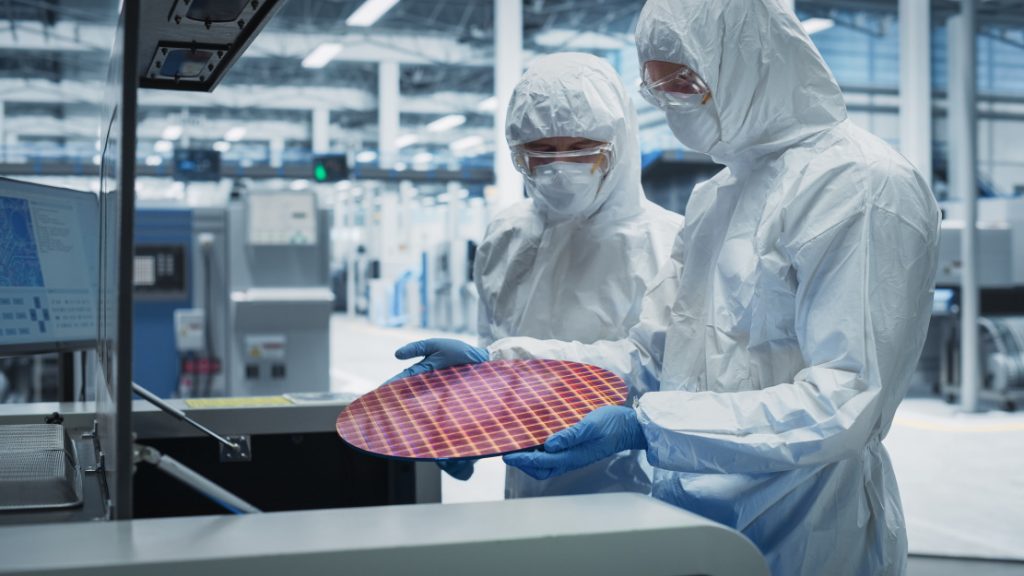
Computer chips and the semiconductors they are made from are getting progressively smaller and more sophisticated. Manufacturing techniques get complicated at tiny sizes, but biology could provide a solution. After all, evolution has had billions of years to perfect construction at the nanoscale. Professor David Estrada, of Boise State University, and Associate Professor Francis Cartieri, of the Community College of Allegheny County, in the US, are investigating the unique properties of DNA, and how they could be harnessed to usher in groundbreaking nanotechnology techniques.
Talk like a nanotechnology engineer
2D structures — a sheet-like, two-dimensional material with a thickness of less than a few nanometres
DNA — the self-replicating molecule that carries genetic information in most living organisms
Nanofabrication — the process of creating structures and devices at the nanoscale
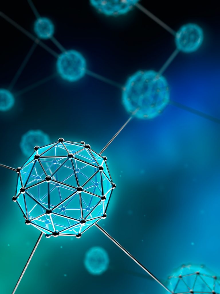
Nanotechnology — the branch of science and engineering that manipulates atoms and molecules at nanoscale to make specialised structures, devices and systems
Neuromorphic computing — a method of computer engineering that creates computer elements modelled on systems in the human brain
Semiconductor — a solid substance with a conductivity between that of an insulator and a conductor, whose conductivity varies according to its impurity levels
Nanotechnology involves the manipulation of substances at the nanoscale – a scale so tiny that it often involves the manipulation of individual atoms. Nanotechnology techniques are highly sophisticated and are continuing to emerge and be refined as scientific understanding improves. However, these techniques are often highly expensive and complicated, which limits their application.
With colleagues at the University of Pittsburgh, the University of Washington and Eastern Washington University, Professor David Estrada, of Boise State University, and Associate Professor Francis Cartieri, of the Community College of Allegheny County, believe that it is time to look to subcellular biological processes for inspiration to make these techniques more effective and accessible. “Back in the 1950s, the celebrated physicist Richard Feynman was one of the first scientists to imagine using biological approaches to miniaturise computing architectures,” says David. “At the time, his ideas seemed like science fiction, but now technology exists that can explore this possibility.” The team is investigating whether biological molecules like DNA could be integrated with semiconductor materials to manipulate matter at the atomic scale, which could open exciting new frontiers for computing power.
DNA nanotechnology
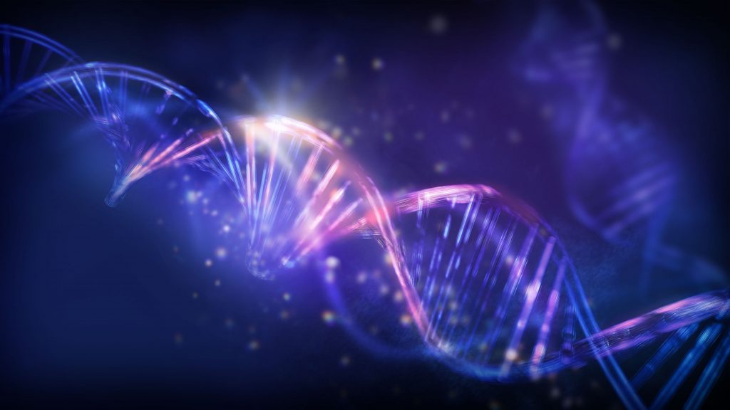
DNA is the molecule that holds all our genetic information within almost every cell. Its structure involves pairs of chemical bases connected in sequence via a double helix. Most importantly for nanotechnology, DNA self-assembles. The bases that make up its sequence pair only with their complementary bases, meaning that single unpaired strands with specific sequences can naturally progress to a full DNA molecule with a pre-defined, predictable shape. “DNA nanotechnology leverages the self-assembly properties of DNA molecules to create nanoscale structures and devices,” explains David. “This involves designing and assembling DNA strands for purposes ranging from medical diagnostics and treatments, through to computation and information storage.”
DNA nanotechnology is a very young field, and its applications are only just beginning to move beyond research labs. The semiconductor industry, in particular, is very interested in its potential. “DNA self-assembly could present a powerful nanofabrication technique,” says Francis. “It could be used to modify materials with molecular precision, enabling the precise manipulation of semiconductors which currently relies on extremely expensive instruments.” As well as bringing down costs, this technique could help bring about next-generation technologies. “In particular, it has applications for brain-inspired neuromorphic computing,” says David. “This type of computing consumes less energy than traditional processors and can be used for AI technologies such as deep learning neural networks.”
DNA can be integrated into nanotechnology through the creation of DNA nanostructure templates, which are precisely-designed DNA strands that interact with each other to create a certain shape – often assembled using a technique known as DNA origami. “This technique involves both long, single strands of DNA and short ‘staple strands’,” explains David. “The short strands find their complementary base pairs on the long strands, and the binding forces involved fold the long strands into the specific shapes we want.” These shapes provide the scaffolds for adding other nanomaterials in a highly controlled manner, potentially overcoming existing challenges around precision and avoidance of defects in the semiconductor industry.
Bringing in 2D materials
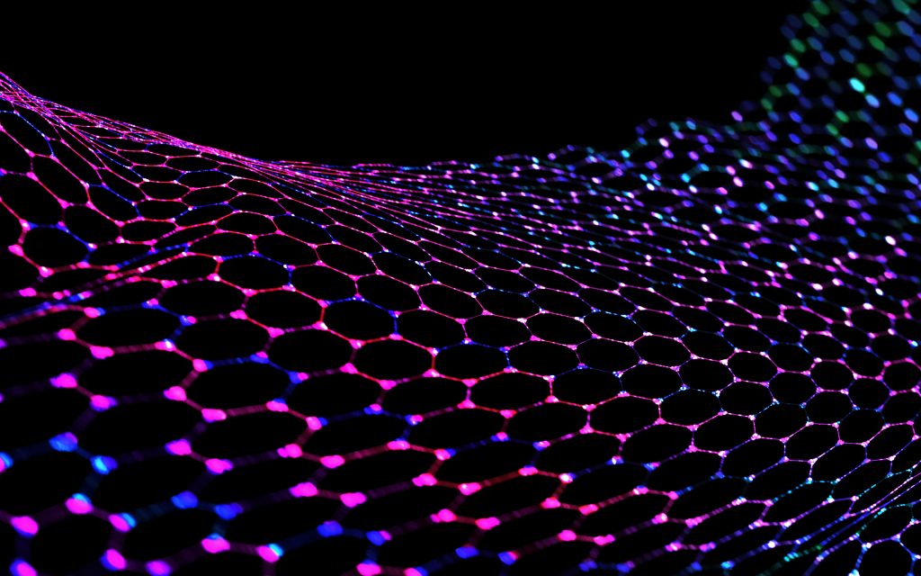
In nanotechnology terms, two-dimensional (2D) materials are typically between one and three atoms thick. “The physical and chemical properties of 2D materials are greatly affected by their chemical composition, crystal structure, and surrounding environment,” says Francis. “This includes their ability to carry electrons – making them of interest for semiconductor manufacture.” Computing relies on semiconductors: the components whose ability to carry charge changes dramatically based on its environmental conditions, which allows for highly complex, fine-scale ‘webs’ of circuits that form the foundation of computational power. Because they can transfer electron charges faster and more efficiently, 2D materials could be viable alternatives to silicon, currently the most widely-used semiconductor material.
David, Francis and the team are aiming to bring together DNA nanotechnology and 2D materials to develop new energy-efficient semiconductors for neuromorphic computing. “If successful, these developments could dramatically reduce the global energy demands of computing,” says David. “We are combining experiments and computation to understand how we can combine and develop these technologies.” The project demands a wide range of expertise and disciplines, and the team is spread across different institutions and time zones. “Learning the vocabulary of different disciplines and establishing effective communication were certainly challenges,” says Francis. “But we have made excellent progress by bringing this community together.”
Reference
https://doi.org/10.33424/FUTURUM611

The team’s progress includes advancements in synthesising 2D materials, as well as using simulations to understand how DNA interacts with 2D materials. “We have published some of our results and have developed various learning modules and short courses for students across our five institutions,” says David. “Next, we’ll be working on how to apply repeatable and precise DNA patterns on our 2D materials, to illustrate the scalability of our approach.” Through an iterative process like this – modelling, testing, modelling again – the team will progressively calibrate their models and develop a deeper understanding of the process, moving ever-closer to applying it to neuromorphic computing.
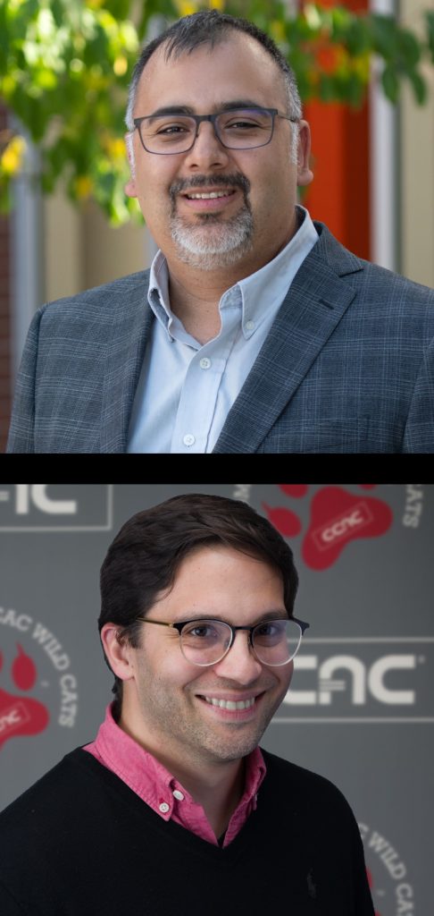 Professor David Estrada
Associate Director, Center for Advanced Energy Studies;
Advanced Manufacturing Deputy Director of Academic Research, Idaho National Laboratory;
Site Director, NSF IUCRC Center for Atomically Thin Multifunctional Coatings (ATOMIC);
Professor, Micron School of Materials Science and Engineering, Idaho, USA
Associate Professor Francis Cartieri
Associate Professor of Mechatronics and Entrepreneurial Manufacturing, Community College of Allegheny County (CCAC), Pittsburgh, Pennsylvania, USA
Field of research: Nanotechnology
Research project: Drawing on DNA nanotechnology and 2D materials to establish new semiconductor manufacturing techniques
Funder: US National Science Foundation (NSF) Award# 2235294
About nanotechnology
Nanotechnology works at the very small nanoscale – the level of molecules, atoms and subatomic particles. Technologies that work at such a precise scale have a diverse range of applications, particularly in computing, where advances in nanotechnology have driven the explosion in global computing power.
Nanotechnology requires a high level of collaboration across disciplines. “Nanotechnology research draws heavily on materials science, physics, chemistry, chemistry, biology, engineering and computer science to name a few,” explains Francis. “It touches all aspects of science and engineering – just at the nanoscale.”
Nanotechnology is a rapidly advancing field, as new applications are continuously discovered and developed. “The future nanotechnology workforce will need a blend of highly technical skills, creativity, and interpersonal and communication skills,” says David. “The adoption of advanced manufacturing technologies and the global uptake of AI demands versatility in the sector, where continuous training and skills development helps workers maintain a competitive edge.”
In terms of emerging research avenues: “The sky’s the limit!” says Francis. “From quantum computing to AI in manufacturing, materials modelling and materials synthesis, there will be ample research opportunities for the next generation.” Impacts of these advances are highly diverse, with promising applications for fields like medicine, manufacturing, the environment, and space science.
Pathway from school to nanotechnology
David and Francis highlight the importance of building a strong understanding of mathematics, physics and chemistry at school.
At university, relevant courses include materials science and engineering, quantum mechanics, and organic and physical chemistry. David also notes the emergence of courses on AI, as well as engineering courses specifically connected to nanoscience and technology.
Explore careers in nanotechnology
David and Francis recommend seeking out professional societies that have nanotechnology-related programmes. These include:
The Institute of Electrical and Electronics Engineers
The Biomedical Engineering Society
The Materials Research Society
The Pathways to Science directory signposts a broad range of US-based opportunities in nanotechnology for high school and undergraduate students, including summer camps and internships.
CareerExplorer provides a useful overview of what a nanotechnology engineer does and explains the different types of nanotechnology engineering roles.
Meet David
Before college, I served for six years in the US Navy as a technician and operator. This developed my interest in electrical engineering, while also allowing me to travel the world. Through visiting numerous countries, I witnessed first-hand the power of education to change life trajectories. It motivated me to pursue a college education and find a field where I can create knowledge that serves humankind.
I got interested in nanotechnology while studying semiconductor devices as an undergraduate. This motivated me to pursue a doctoral degree, which introduced me to 1D and 2D nanomaterials. These days, I am interested in their application not only for semiconductors, but also within the energy, environmental and healthcare sectors.
We have a very interdisciplinary team environment in my lab. Students are from disciplines including biomolecular sciences, biomedical engineering, electrical engineering, materials science and physics. This range of perspectives enables the team to bring tools from different disciplines to solve problems collectively. It’s always fun to see the team work together and find creative solutions, or devise new applications for their discoveries.
I’ve worked with NASA, the Department of Energy and the US Air Force to develop new materials for printed electronics. We helped NASA screen materials printers for future missions, helped create new sensors and devices for national defence, and even deployed printed sensors into the core of nuclear reactors.
I really want the materials and devices we design to have a major impact on our lives. Whether it’s microelectronics for fusion and fission reactors, data sensors for the extremes of space, or circuits that mimic the human brain, I’m excited to work across disciplines to realise the next generation of materials and microelectronics.
David’s top tips
Study hard, work hard, and be kind.
Meet Francis

So much of the world only makes sense when you look at it at very small scales. The iridescent blue of butterfly wings only makes sense under an electron microscope. Only then can we see that it’s the structure, not the substance, that creates that dazzling colour. This is why I love working at the intersection of biology and robotics.
One ‘eureka’ moment of my career was while working for a cancer surgeon. We were trying to develop cost-effective artificial skin tissue, but skin has a very complicated nanoscale structure that is hard to mimic from scratch. I borrowed some ideas from textile manufacturing to make a nanoscale threaded fabric that worked like a template. Under the right conditions, biological material dissolved and replaced the template. When I first saw the results under an electron microscope, I couldn’t believe it worked!
I have a compulsion to keep learning all the time. I chose an occupation that rewards that. To stay curious and thoughtful, I still find it helpful to switch off from all screens, my phone included.
Francis’s top tip
Find potential mentors: people that are doing what you want to be doing. Talk to them and ask them about their work.
Do you have a question for Francis and David?
Write it in the comments box below and Francis and David will get back to you. (Remember, researchers are very busy people, so you may have to wait a few days.)

Read about how Francis and colleagues are bringing low-cost nanofabrication learning techniques into schools and colleges:
futurumcareers.com/turbocharging-nanofabrication-skills-for-an-automated-society
The post Harnessing DNA to make cutting-edge nanoscale semiconductors appeared first on Futurum.
“}]]

